[previous] [next] [contents]
![]() Boundary-scan
test - The instruction register
Boundary-scan
test - The instruction register
The IEEE 1149.1 std defines mandatory and optional instructions, respectively addressing (or selecting) the mandatory and optional data registers shown in the BS architecture depicted in figure 1.
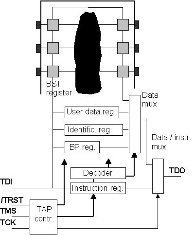
Figure 1: The BS architecture at IC level.
The mandatory instructions are those guaranteeing the basic objectives underlying the development of the BS test technology and may be briefly described as follows:
The EXTEST instruction selects the BS register and imposes the (external) test mode in each BS cell, decoupling the IC core logic from the pins. The configuration shown in figure 2 for a BS cell will however enable internal tests to be carried out as well, since the BS cells associated to input pins may be used to apply test vectors and the BS cells associated to output pins used to capture the responses. The EXTEST instruction has a pre-defined code of all-0s.
- The SAMPLE / PRELOAD instruction also selects the BS register, but the BS cells are now in transparent mode. The main objective of this instruction is to enable a first vector to be shifted in before the internal logic is decoupled from the pins (while the BS cell output latches are not loaded with meaningful data, it may be necessary to prevent their initial value to appear on the parallel output of the cell). This instruction does not have a pre-defined code.
- The BYPASS instruction selects the bypass register and enables a 1-bit data path through those ICs which do not play a role in the current test operation. This instruction has an all-1 code and is automatically loaded into the instruction register on reset (the BS register will in this case have its cells in transparent mode, meaning that at power-up all BS ICs will start to perform their normal functions).
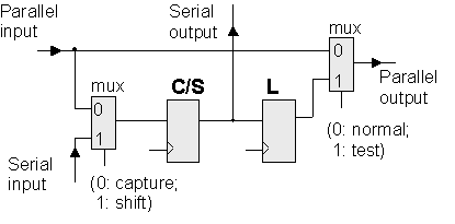
Figure 2: Typical BS cell configuration.
A number of optional BS instructions are possible with the objective of supporting other test operations or the optional data registers shown in figure 1. The description of these instructions will be present in the device datasheet, but the IEEE 1149.1 std defines a few possible instructions, including the following:
- The IDCODE selects the identification register and enables access to a unique 32-bit code identifying the device manufacturer, the part number and the version number.
- User-programmable components may also support an USERCODE instruction that selects the same 32-bit identification register, now with the objective of enabling access to a user-programmable identification code.
- The RUNBIST instruction is used to enter a self-test mode that leaves the test result in the data register selected by this instruction (a dedicated user test data register will normally be used for this purpose).
None of the optional instructions have pre-defined codes. The optional instructions to support are naturally left to the discretion of the designer and it is possible that a BS component supporting several optional instructions does not support those referred above (such as is the case with the SCOPE octals manufactured by Texas Instruments).