[previous] [next] [contents]
![]() Boundary-scan
test - The test data registers
Boundary-scan
test - The test data registers
Figure 1 shows that the n:1 data multiplexer enables the choice of which data register to place between TDI and TDO, according to the instruction currently present in the instruction register. From none to several "User data registers" may exist, bringing the total number of data registers to a minimum of three and to a maximum that depends only on the testability infrastructures which the designers cared to insert.
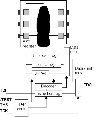
Figure 1: The BS architecture at IC level.
A brief description of each of the data registers shown above may be presented as follows:
- The BS register comprises the set of BS cells present in the circuit and is mandatory in any BS IC. The main function of this register is to apply test vectors and capture test responses, essentially at PCB-level (and eventually also at IC level, as was previously referred). At least two instructions selecting this register have to be supported (EXTEST and SAMPLE / PRELOAD).
- The bypass register is another mandatory register defined in the IEEE 1149.1 std and its function is to shorten the total length of the serial PCB-level chain, when the scan operation addresses only a subset of the ICs present. This register is 1-bit long and is selected by the BYPASS instruction, which is also always supported.
- The identification register is optional and its function is to provide a 32-bit sequence enabling the test engineer to perform an identity check on each device supporting the IDCODE instruction.
- The user test data registers are also optional and will normally interface additional testability infrastructures introduced by the designers. An example could be the register storing the result of BIST (Built-In Self-Test) operations.
There is a close relationship between the data registers and the instructions supported, since each instruction selects one data register (and a particular operating mode, if more than one instruction select the same register).