[previous] [next] [contents]
![]() Basic test concepts -
Redundancy and undetectable faults
Basic test concepts -
Redundancy and undetectable faults
Low testability may lead to undetectable ss@ faults, whenever it becomes impossible to simultaneously activate a fault and propagate the error signal to a primary output. The circuit shown in figure 1 will help us to understand this class of faults, by considering the case of node X s@0.
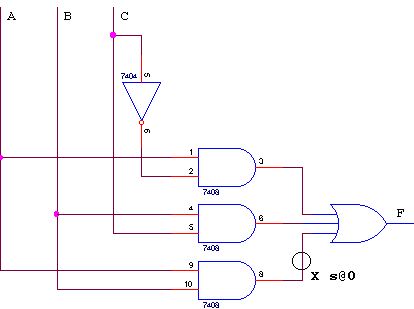
Figure 1: A simple combinational circuit with an undetectable fault (X s@0).
The circuit shown may be represented in its sum-of-products form by the expression F = A*/C + B*C + A*B, which corresponds to the K-map represented in figure 2.
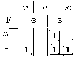
Figure 2: K-map corresponding to the circuit shown in figure 1.
The K-map representation brings into evidence that the product term A*B
is redundant, since all the 1-cells were already covered by the other
two product terms. If we remove the redundant term A*B, the resulting
circuit shows itself as the standard implementation of a 2:1 multiplexer,
where C is the control input, and A and B are the data inputs. There is
no test vector able to detect the s@0 fault at the output of the redundant
product term (node X), because the necessary condition to activate this
fault (A=B=1) will also prevent its propagation, by setting one of the
remaining OR inputs to 1. As stated above, it is not possible to simultaneously
activate the fault and propagate the error signal.
Redundancy is a major cause of low testability, but it is used deliberately
in various situations. Spatial redundancy (i.e. the hardware replication
of functional blocks) is in fact the basis of a common form of fault tolerant
architectures, known as N-modular redundancy (of which TMR, triple modular
redundancy, is the simplest implementation). N-modular architectures use
N functional replicas in parallel and a voter circuit that performs a
majority vote to determine the output. If a faulty replica produces an
incorrect output, it will be masked by the voter circuit. Fault masking
guarantees that the circuit performs well in the presence of single faults,
which in other words become undetectable, as far as common test vector
generation algorithms are concerned.
The case of figure 1 is however different, since this multiplexer does
not possess any fault tolerant features. In fact, the redundant product
term A*B is present with the sole objective of avoiding the possible occurrence
of output glitches, shown in figure 3.
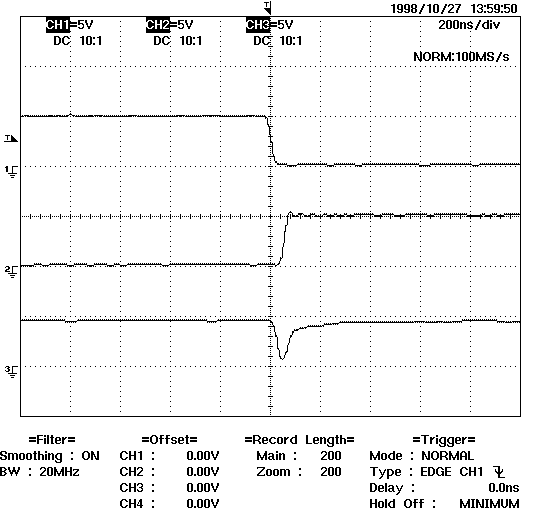
a) Waveforms: inverter input C, inverter output /C and output F.
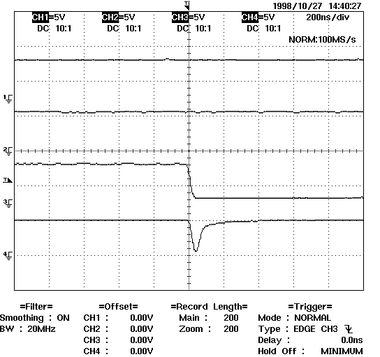
b) Waveforms: inputs A, B, C, and output F.
Figure 3: Glitch at the outputs of a standard 2:1 multiplexer (implemented with two product terms).
The propagation delay of the inverter causes the two upper AND gates
in figure 1 to have a 0 applied simultaneously to their lower inputs,
during a short time interval, whenever input C descends. Depending on
the propagation delay of the inverter, the output of a standard 2:1 multiplexer
(i.e. one with only two product terms) may exhibit the glitch shown in
figure 3-a), where the waveforms at C, /C and F are represented. Notice
that inputs A and B are both at 1 on figure 3-b), but the standard 2:1
multiplexer considered still produces a low-level glitch at the output
(the waveforms represented are respectively A, B, C and F). Product term
A*B was added to prevent this problem, since it guarantees that at least
one of the OR inputs will always be at 1, whenever A and B are both at
1. However, while solving a time domain problem, the redundant product
term created a testability problem.
The example presented also shows that node X s@0 is undetectable only
as far as our static test vector generation algorithm is concerned.
In fact, since X a@0 will enable the output glitch shown in figure 3,
this fault may be detected if we analyse the transient response of
the circuit.