[previous]
[contents]
![]() Proposed
experiments with the 1149.4 "component"
Proposed
experiments with the 1149.4 "component"
The
wire-wrapping prototype previously described will be used to carry out two
main basic experiments, addressing the concepts of observability and
controllability in the mixed-signal test domain:
-
Observability: the waveform at the analog output pin will be observed at AT2, when the analog input (and therefore the analog output as well, since the internal circuitry consists of a simple voltage follower) is driven by a sine wave
-
Controllability: the waveform at the analog output pin will be driven from AT1 (a square wave), regardless of what signal is applied at the analog input (the sine wave, in this case)
The PROBE
instruction is used to carry out the observation experiment. The following
conditions will be set up, as shown in figure 1: core connected to the pin
at both ABMs, pin connected to AB2 at the output ABM and AT2 connected to
AB2.
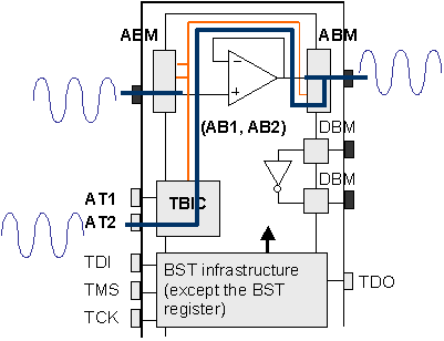
Figure
1: Test set up for the
observability experiment.
The following
test program, written for the Tapper application, sets the required
operating mode for the test circuitry:
TRST
TMS1
TMS1
TMS1
TMS1
TMS1
; Test Logic Reset
; ANALOG PINS CONNECTED TO CORE AND ISOLATED FROM ALL
; TEST CIRCUITS
TMS0
; Run-test/Idle
TMS1
; Select-DR
TMS1
; Select-IR
TMS0
; Capture-IR
TMS0
; Shift-IR
LD
C16, 8
NSHFCP
$02,$01,$FF
; 00000010 00000001 11111111
JPE
FIM
TMS1
; Update-IR - Sample/Preload
TMS1
; Select-DR
TMS0
; Capture-DR
TMS0
; Shift-DR
LD
C16, 14
NSHF
$04, $04 ; LSB is 1st
to be shifted
; xx 0001 0000 0001 00
; xx TBIC ABM
ABM DBMs
TMS1 ;
Update-DR
TMS1
; Select-DR
TMS1
; Select-IR
TMS0
; Capture-IR
TMS0
; Shift-IR
LD
C16, 8
NSHFCP
$01, $01, $0FF
JPE
FIM
TMS1
; Update-IR - PROBE
;
AB1 CLAMPED; AB2 CONNECTED TO AT2
; ANALOG INPUT PIN CONNECTED TO CORE AND ISOLATED FROM
; ALL TEST CIRCUITS
; ANALOG OUTPUT PIN CONNECTED TO CORE AND MONITORED BY AB2
FIM: HALT
.END
The waveforms
observed at the analog pins and the ATAP are shown in figure 2, before and
after execution of the test program segment presented above.
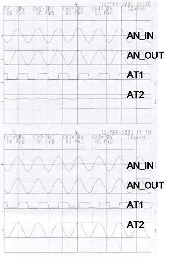
Figure
2: Observability
experiment waveforms.
The EXTEST
instruction is used to carry out the controllability experiment. The
following conditions will be set up, as shown in figure 3: core
disconnected from the pin at the output ABM, pin connected to AB1 at the
output ABM and AT1 connected to AB1 (the connection between pin and core
at the analog input is not relevant). We’ll start with the analog output
disconnected from AB2, and will then establish this connection as well,
enabling simultaneous controllability and observability at the analog
output pin.
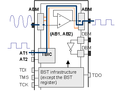
Figure
3: Test set up for the
“controllability” experiment.
The following
Tapper test program sets the required operating mode of the test
circuitry, for this experiment:
TRST
TMS1
TMS1
TMS1
TMS1
TMS1
; Test Logic Reset
; AB1/2 DISCONNECTED FROM AT1/2 AND CLAMPED
; ANALOG PINS CONNECTED TO CORE AND ISOLATED
FROM
; ALL TEST CIRCUITS
TMS0
; Run Test / Idle
TMS1
;
Select-DR
TMS1
; Select-IR
TMS0
; Capture-IR
TMS0
; Shift-IR
LD
C16, 8
NSHFCP
$02,$01,$FF
; 00000010 00000001 11111111
JPE
FIM
TMS1
; Update-IR - Sample/Preload
TMS1
; Select-DR
TMS0
; Capture-DR
TMS0
; Shift-DR
LD
C16, 14
NSHF
$08,$08 ; LSB is 1st to be
shifted
; xx 0010 0000 0010 00
; xx TBIC
ABM ABM DBMs
TMS1
; Update-DR
TMS1
; Select-DR
TMS1
; Select-IR
TMS0
; Capture-IR
TMS0
; Shift-IR
LD
C16, 8
NSHFCP
$00,$01,$FF
JPE
FIM
TMS1
; Update-IR - EXTEST
; AB1 CONNECTED TO AT1; AB2 CLAMPED
; ANALOG INPUT PIN COMPLETELY ISOLATED
(CD STATE)
; ANALOG OUTPUT PIN CONNECTED TO AB1
TMS1
; Select-DR
TMS0
; Capture-DR
TMS0
; Shift-DR
LD
C16, 14
NSHF
$0C,$0C ; LSB is 1st
to be shifted
; xx 0011 0000 0011 00
; xx TBIC
ABM ABM DBMs
TMS1
; Update-DR
; AB1/2 CONNECTED TO
AT1/2
; ANALOG INPUT PIN
COMPLETELY ISOLATED
; ANALOG OUTPUT PIN
CONNECTED TO AB1 AND MONITORED BY AB2
FIM: HALT
.END
The waveforms
observed at the analog pins and the ATAP are shown in figure 4, before and
after execution of the test program segment presented above.
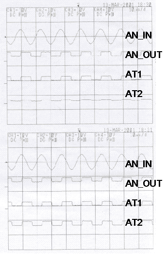
Figure
4: Controllability
experiment waveforms.
What should be the contents of the BS register, assuming PROBE as the current instruction, in order to enable the observation of the analog output pin at AT2? (the rightmost bit is shifted in first).