[previous] [next] [contents]
![]() Implementation
of the 1149.4 demo "component"
Implementation
of the 1149.4 demo "component"
The
implementation technology should meet three main objectives: be widely
available, be flexible (to enable modifications / upgrades, if required)
and be pedagogical (i.e. make explicit the operation of the internal test
circuitry). The best alternative, requiring a relatively small number of
IC packages, consists of implementing the digital test infrastructure and
core logic in an EPM7128 Altera PLD (2.500 usable gates, 128 macrocells,
84-pin PLCC), and using discrete components to implement all the remaining
blocks (ADG452 analog switches, LM311 comparators, TL081 operational
amplifier).

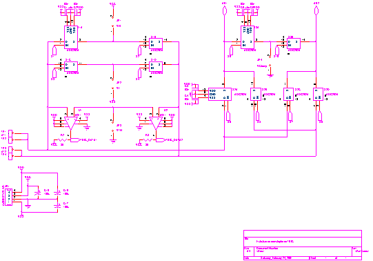
Figure
1: Top-level
representation of the digital test infrastructure and core (logic
inverter).
The digital test infrastructure and core logic (simply a logic inverter) was implemented by Dr. Gustavo Alves of ISEP and is illustrated in figure 1, which lists all input / output signals that interface the remaining (analog) blocks. This block was designed using the Max+plus II Baseline software, where a schematic representation was selected for the upper hierarchical levels – the top level is shown in figure 2 -, and a hardware description language (AHDL) representation for the lower levels.
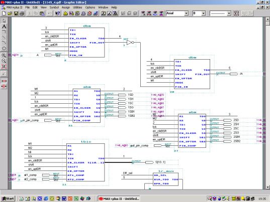
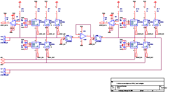
Figure
2: Max+plus II -
Top-level representation of the digital test infrastructure and logic
inverter.
Each block
represented in figure 2 will either be described directly in AHDL, if no
intermediate hierarchical levels are present, or by a further breakdown of
blocks, represented in schematic diagram form, which are then described in
AHDL. As an example, figure 3 shows the representation of each ABM, which
comprises a (4-bit) control register and a decoder (generating the control
signals for the analog switches).
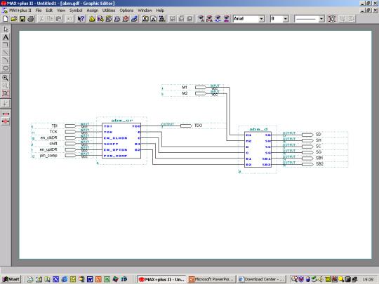
Figure
3: Schematic
representation of the digital circuitry comprised in each ABM.
Each block
represented in figure 3 is then described in AHDL. This hardware
description language provides a very straightforward representation of the
required logic functions, as may be seen by analyzing the section that
refers to the ABM control structure, shown in figure 4.
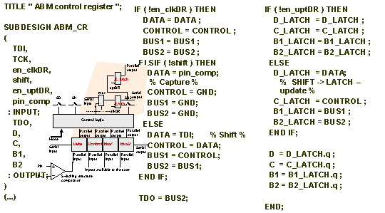
Figure
4: AHDL representation of the ABM control structure.
The ABM
switching decoder provides another good example of the readability of AHDL.
Figure 5 shows that this combinational circuit was specified in the form
of a table, where each line represents the input / output relationship
required for each switching pattern.
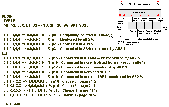
Figure
5: AHDL representation of
the ABM switching structure decoder.
The
implementation of the switching structures of the TBIC and ABMs is based
on discrete components, as was previously referred. Figure 6 shows the
schematic diagram representation of the TBIC switching structure, which
uses ADG452 analog switches and LM311 open-collector output comparators.
Figure
6: Implementation of the
TBIC switching structure.
The switching
structure of the ABMs uses the same components and is represented in
figure 7, together with the internal core circuitry (the voltage
follower).
Figure
7: Implementation of the
ABMs switching structure.
The whole
1149.4 “component” was assembled in a printed circuit board that is
shown in figure 8.
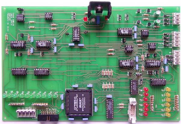
Figure
8: The 1149.4 demo
“component”.