[previous] [next] [contents]
![]() The
Test Bus Interface Circuit (TBIC)
The
Test Bus Interface Circuit (TBIC)
The basic architecture of 1149.4, illustrated in figure 1, shows that two main blocks were added to the original 1149.1 test infrastructure, respectively the TBIC and the ABMs. These blocks assure the main feature of 1149.4, which is the application and monitoring of analog test signals. Each of these blocks comprises a switching structure (defining the interconnection among their I/O signals) and a control structure (which defines the operating mode of the switching structure), that will now be analysed in detail.
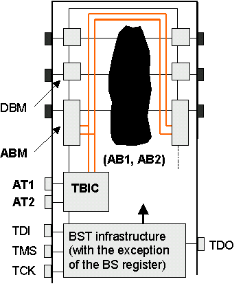
Figure 1: The basic 1149.4 architecture.
The TBIC controls the connections between the ATAP and the internal analog test lines. The 1149.4 document specifies that there must be at least two internal analog test lines, AB1 and AB2, as was shown in figure 1.
TBIC - The Switching Structure
Figure 2 represents the switching structure of the TBIC, assuming that the internal analog test bus comprises two lines, AB1 and AB2.
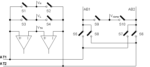
Figure 2: Switching structure of the TBIC.
The ten switches shown in figure 2 (S1 to S10) define the signals that will be present in the ATAP pins and the internal analog test bus lines. Notice in particular that the switching structure of the TBIC allows:
- AT1 / AT2 to be connected to VH / VL
- AT1 / AT2 to be connected to AB1 / AB2
- AT1 / AT2 to be connected to the internal voltage source VCLAMP
- A 1-bit representation of the voltage at AT1 or AT2 (as compared to the threshold voltage VTH)
The state (on / off) of the switches shown in figure 2 is defined by the TBIC control structure. Since not all possible combinations are useful (or legal), four bits are sufficient to select the required operating mode, as illustrated in figure 3 (the current draft specification describes only ten switch combinations, which are able to satisfy the basic requirements set up for the TBIC).
TBIC - The Control Structure
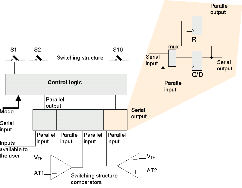
Figure 3: Control structure of the TBIC.
The TBIC control structure forms part of the BS register and its description may be summarised as follows:
- It comprises four cells (bits), each one with a capture / shift stage and an update stage. Notice that these cells are not significantly different from the typical configuration found in standard 1149.1 BS cells. The main difference is the absence of an output multiplexer, which is not required here because these cells have no external parallel input.
- The four bits in the capture / shift stage are called CALIBRATE, CONTROL, DATA1 and DATA2. DATA1 and DATA2 capture the 1-bit representation of the voltages at AT1 and AT2, as compared to VTH, while CALIBRATE and CONTROL are available as additional capture inputs for design-specific circuit conditions.
The four bits in the update stage, together with the instruction decoder outputs MODE1 and MODE2, define the operating mode of the TBIC switching structure.