[previous] [next] [contents]
![]() Scan
design techniques - Structured approaches to DFT
Scan
design techniques - Structured approaches to DFT
The basic concept underlying most structured design for testability (DfT)
methodologies consists of providing a systematic way of forcing the circuit
to any given state in a fixed (and short) number of clock cycles, regardless
of the current state and of the fault present in its combinational circuitry
(even if affecting the next-state generation logic). The expression structured
DfT implies that the same design approach can always be used and assure
good testability levels, regardless of the circuit function. There is
however a price to pay, which normally consists of accepting that some
design rules (rather a design style) are enforced and that additional
silicon area and propagation delays are tolerated.
The test vector generation problem can be greatly simplified for any synchronous
sequential circuit built with D flip-flops (D-FF), if each D-FF input
is preceded by a 2:1 multiplexer, with all multiplexers sharing a common
control signal. This scheme is shown in figure 1, where we can see that
forcing a 1 at the Test Mode control signal will rearrange all
D-FFs in a standard shift-register and will enable any state combination
to be shifted in using exactly N clock cycles (with N being the number
of D-FFs).
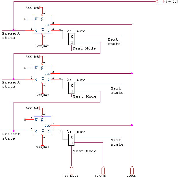
Figure 1: Scan design principle.
When each D-FF in the circuit is preceded by this 2:1 multiplexer (creating what is commonly called a scan flip-flop) we have a case of full-scan design. This structured DfT methodology started to gain wide acceptance in the late 70s, when it became evident that test vector generation algorithms for sequential circuits would not be able to cope with the increasing complexity of emerging VLSI designs. Scan design techniques overcome this difficulty by providing a simple solution to the two main problems that make test vector generation for sequential circuits so much complex:
First problem: Part of the combinational circuitry inputs are
not directly controllable, since they come from the D-FF outputs (these
nodes define the circuit present state).
Solution: The scan flip-flops shown in figure 1 enable direct controllability
of the D-FF outputs through a simple procedure with a fixed number of
clock cycles:
- Set the Test Mode control signal to 1
- Shift in the required state combination (three clock cycles)
- Set the Test Mode control signal to 0
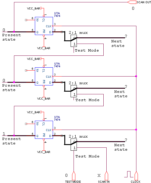
Figure 2 shows the example of taking the circuit to state 110,
assuming that the current state was 100 and that the next state
inputs were 001 (notice again that this sequence is always possible,
regardless of the whatever function the circuit performs or wherever the
fault s@ is located):
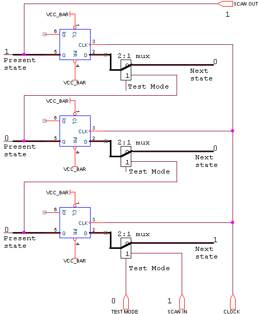
(a)
Initial circuit conditions: Present state 100, next state 001.
Recall that the present state nodes are (internal) inputs of the combinational
logic block defining the global sequential circuit function and that the
next state nodes are (also internal) outputs of this same block.
Since the Test Mode control signal is at 0, each clock cycle will
transfer to the D-FFs outputs the values present at the next state nodes.

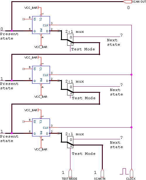
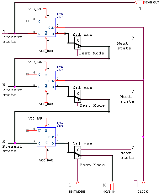
(b)
The Test Mode control signal is now at 1 and the D-FFs are connected
as a shift-register. The first clock cycle applied will shift the D-FFs
one bit position "up" and transfer the value present at the
Scan In input to the output of the first D-FF in the chain.
The values shown at each node are those following the application of the
first clock cycle with Scan In at 1. Notice that the next state
values will now be different from the initial conditions, since the inputs
of the combinational block now have different values as well.
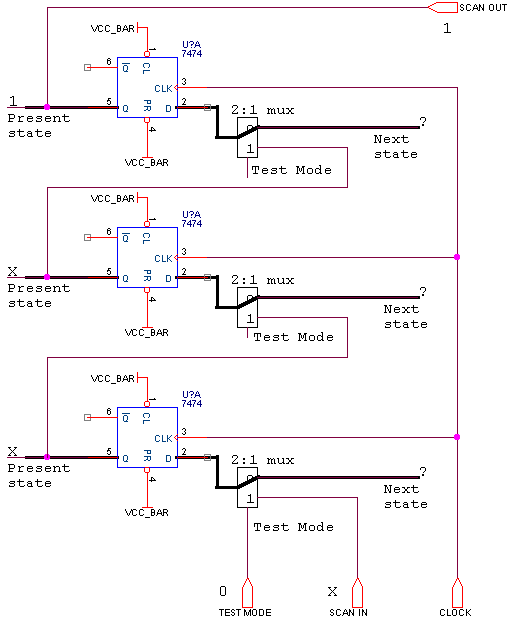
(c)
The values shown at each node are now those following the application
of the second clock cycle, keeping Scan In at 1.
Notice that the initial present state values are being shifted out simultaneously
as the new present state is being shifted in, even if we are only interested
in shifting a new combination into the present state nodes.

(d)
The last clock cycle has now been applied with the Scan In input set
at 0, so the new present state is 110 as requested.
Three clock cycles were therefore necessary to take the circuit to its
new present state, the general rule being that the number of clock cycles
required is equal to the number of D-FFs. For larger circuits this rule
guarantees a much faster transition to any given state (in the extreme
case, for a circuit with N D-FFs, 2N-1 clock cycles are replaced
by N clock cycles).
(e)
The requested present state has been loaded and the Test Mode control
signal has been taken back to 0.
Each next state node is now connected to the respective D-FF input and
is defined by the combinational logic block according to present state
110 and to the current values at the (external) sequential circuit
primary inputs
Figure 2: Controllability of the present state nodes.
Second problem: Part of the combinational circuitry outputs are
not directly observable, since they go to the D-FF inputs (these nodes
define the circuit next state).
Solution: The scan flip-flops shown in figure 1 enable direct observability
of the D-FF inputs through a similar procedure:
- Capture the values present at the D-FF inputs (the outputs of the combinational circuitry)
- Set the Test Mode control signal to 1
- Shift out the required state combination (three clock cycles)
- Set the Test Mode control signal to 0.
Figure 3 considers the same initial conditions as in figure 2.(a) and
shows how to observe the next state defined by the combinational circuitry
outputs (again whatever the circuit function, wherever the fault may be):

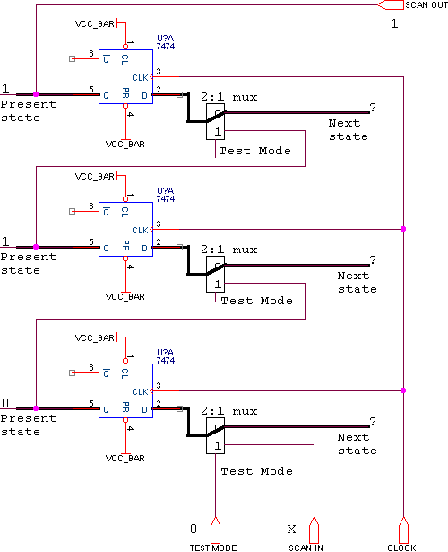
(a)
The initial circuit conditions are the same as in the previous example,
the present state being 100.
The 2:1 multiplexers have their Test Mode control signal at 0 and
are therefore in "transparent" mode (apart from the larger propagation
delay, the circuit behaves as if no DfT techniques were present).
(b)
The values shown at each node are those following the application of
the first clock cycle. Since the Test Mode control signal was kept at
0, the values transferred to the D-FF outputs were those present
in the next state nodes, defined by the (internal) outputs of the combinational
logic block. Notice that the value present at the Scan Out output is now
the first bit (leftmost) requested to be shifted out.
As was seen in the previous example, the next state node values have been
modified as well.

(c)
The Test Mode control signal was now set to 1 and the values shown
at each node are those following the application of the second clock cycle.
Since the D-FFs are now connected as a shift-register, the present state
nodes were shifted one bit position "up" and the second bit
was shifted out.
Notice that the first D-FF in the chain loads the value present at the
Scan In input, even if we are not interested in controlling the values
to be left at the present state nodes in the end.
(d)
The values now shown are those following the application of the third
(and last) clock cycle. The last bit (the rightmost bit in the initial
001 next state) was now shifted out.
Notice that only two clock cycles were required after the Test Mode control
signal was set to 1, since the first bit is immediately present
at the Scan Out output.
(e)
Setting the Test Mode control signal to 0 brings the circuit back
to the normal operation mode.
The present state was modified as defined by the values shifted in and
the next state values were modified accordingly. Notice however that the
initial present state might have been kept, if Scan Out and Scan In were
directly connected and a fourth clock cycle was applied before setting
the Test Mode control signal back to 0.
Figure 3: Observability of the next state nodes.
The main virtue of scan design techniques is therefore their ability to eliminate the sequential nature of the circuit, which is seen by the test vector generation tool as a pure combinational circuit. The remarks initially made concerning the cost of DfT should be clear by now:
- The presence of the extra 2:1 multiplexers leads to larger propagation times and requires extra silicon area, eventually increasing the circuit cost. Notice however that we can not be positive about the cost issue, since it might well happen that our circuit had spare pins and was not core-limited, in which case the circuit might actually become cheaper to produce (since test is now so much easier).
- The designer is not free to use whatever solution he might find more appropriate, since the controllability and observability of all combinational inputs and outputs can only be achieved if the synchronous scan flip-flop structures defined by full-scan techniques are accepted for the whole circuit (for example, no asynchronous structures are allowed).
In those cases where full-scan can not be accepted, it is still possible to select only those nodes which present higher testability problems and use scan flip-flops in those circuit areas.