[previous] [next] [contents]
![]() Boundary-scan
test - The BS architecture and test access port
Boundary-scan
test - The BS architecture and test access port
The basic concept underlying the BST technology is shown in figure 1 and consists of associating a dedicated test cell to each functional pin. These test cells are the Boundary Scan cells and their main function consists of decoupling the internal logic from the IC pins, allowing the application of the required logic values at the cell outputs, regardless of the values present at their inputs. It therefore becomes possible to:
- Apply any combination to the IC output pins and to the IC internal logic inputs (through the parallel output of the BS cells).
- Capture the values present at the IC input pins and at the internal logic outputs (through the parallel input of the BS cells).
The serial input of each
cell is connected to the serial output of the previous cell within each IC, forming an
internal chain known as the Boundary Scan Register. Since all BS registers may be
daisy-chained at PCB level, as suggested in figure 1, direct access to any BS pin is now
possible, without requiring physical access to internal PCB nodes.
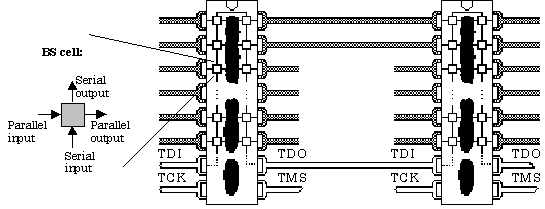
Figure 1: The basic concept underlying the BST technology.
Figure 1 also suggests that additional resources are required in each IC to control the operating mode of the BS cells, leading to a dedicated set of test pins known as the Test Access Port (TAP). This TAP includes 4 pins with the following characteristics, as defined in the IEEE 1149.1 std:
- TDI (Test Data Input): The serial data input to the BS register. When floating, this pin produces a response identical to the application of a logic 1.
- TDO (Test Data Output): The serial data output of the BS register. This is the only output pin in the TAP and must be in the high-impedance state except when a scan operation is in progress.
- TCK (Test Clock): The clock signal for the test logic.
- TMS (Test Mode Select): A control input that defines the operating mode required for the test logic. When floating, this pin produces a response identical to the application of a logic 1.
Optionally, a fifth pin may be present for initialisation purposes (the /TRST ¾ Test Reset, active low ¾ pin). The complete BS architecture may in fact be represented as shown in figure 2, which brings into evidence the following main features:
- The TDI-TDO path goes through two multiplexers, a n:1 "Data multiplexer" and a 2:1 "Data / Instruction multiplexer".
- The 2:1 data / instruction multiplexer is controlled by an output of the "TAP controller" block (which is a small finite state machine controlled by the external input TMS) and selects the TDI-TDO path through the "Instruction register" or one of the "Data registers" (one of which is the BS register).
- The n:1 data multiplexer is controlled by the contents of the instruction register (through a decoder block called the "Instruction decoder") and selects which of the data registers is to be routed to the TDO output, through the data instruction multiplexer.
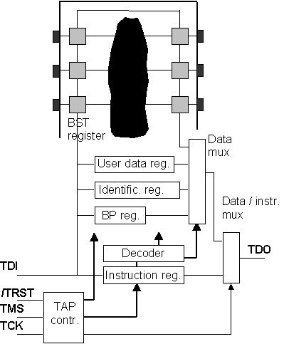
Figure 2: The BS architecture at IC level.
Access to this BS architecture is controlled by the sequence of logic values applied to the TMS input and may be summarised as follows:
- The TAP controller output connected to the data / instruction multiplexer places the instruction register in the TDI-TDO path.
- The proper bit sequence (instruction) is shifted in, setting the contents of the instruction register with the code that selects the required data register (by controlling the n:1 data multiplexer).
- The TAP controller output connected to the data / instruction multiplexer places the selected data register in the TDI-TDO path.
- Test vectors may now be shifted in and out through the selected test data register.
However, and before a block-level analysis of the architecture shown in figure 2 takes place, the basic functional requirements that must be satisfied by the BS cells will be detailed in the following section.