[previous] [next] [contents]
![]() Boundary-scan
test - The basic boundary-scan cell
Boundary-scan
test - The basic boundary-scan cell
The typical BS cell configuration is represented in figure 1 and shows that:
- The output multiplexer (controlled by the Mode signal) enables a transparent mode of operation in which the parallel output is directly connected to the parallel input of the cell.
- The Mode signal controlling the output multiplexer, if set to 1 (Test mode), enables a controllability mode of operation, in which the paralleoutput takes the value present at the output latch, regardless of the value present at the parallel input.
- The Shift signal controlling the input multiplexer, if set to 0, enables an observability mode of operation, in which the value present at the parallel input is sampled into the left flip-flop and may be shifted out (by setting the Shift signal to 1).
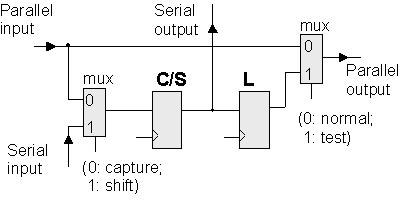
Figure 1: Typical BS cell configuration.
These three basic operating modes of the BS cells enable test operations to proceed according to a simple protocol which consists of the following steps:
- Shift in a new test vector (left multiplexer in Shift mode, right multiplexer in either Normal or Test modes)
- Apply the test vector at the parallel outputs of the cells (left multiplexer in either Shift or Capture modes, right multiplexer in Test mode)
- Capture the responses present at the parallel inputs of the cells (left multiplexer in Capture mode, right multiplexer in either Normal or Test modes)
- Shift out the responses (left multiplexer in Shift mode, right multiplexer in either Normal or Test modes)
Notice that the first and last steps described above may, and do in fact, take place at the same time, since the process of shifting in a new test vector may proceed simultaneously as the responses to the previous vector are shifted out. Notice also that the sequence of steps presented above is the same either for testing interconnects at PCB level or for testing the core logic in a BS IC. However, and since the contents of the selected scan chain have to be shifted in / out for each test vector, this test protocol becomes very slow for large numbers of test vectors. Low speed wouldn’t be acceptable for testing the internal logic of an IC, which may require hundreds of thousands of vectors, but it presents no problems as far as the main application domain of BST is concerned: the structural testing of digital PCBs. As we will see later when considering the detection of open and short-circuit faults in PCB interconnects, only a reduced number of test vectors is required to enable complete fault detection.