[previous] [next] [contents]
![]() Fault
detection in non-BS clusters
Fault
detection in non-BS clusters
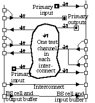
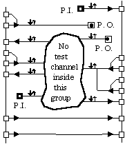
Fault detection in non-BS clusters (groups of non-BS components that are present in boards with BS) might be done exclusively through the surrounding BS components, but smaller test times and higher fault coverage may be achieved if external test resources are available as well. The BS infrastructure and external test channels may be combined mainly as represented in the three cases shown in figure 1.
|
|
|
|
|
(a) Full access. |
(b) Peripheral access. |
(c) Primary I/O access only. |
The symbol ![]() is used in figure 1 to represent an external test channel with direct
physical access to the PCB node. The three situations shown correspond to
different trade off solutions in terms of test speed (and eventually fault
coverage as well) versus cost (in resources of test equipment and physical
access provisions), which may be summarised as follows:
is used in figure 1 to represent an external test channel with direct
physical access to the PCB node. The three situations shown correspond to
different trade off solutions in terms of test speed (and eventually fault
coverage as well) versus cost (in resources of test equipment and physical
access provisions), which may be summarised as follows:
- Full access (figure 1.a) means that the non-BS cluster may be tested independently of the surrounding BS chain, since all interconnects (internal or in the periphery) have an in-circuit test channel. This is the fastest solution (no scan operations involved), but requires extensive test resources and non-restricted physical access, which in many cases will not be possible.
- Physical access to those interconnects in the periphery of the non-BS cluster (figure 1.b) is an alternative which requires less test resources, due to the much lower number of physical access points. The external in-circuit test channels enable a functional test of the cluster, which will normally result in lower test speeds, but which still does not require any scan operations.
- When physical access is not at all possible except to the primary inputs and outputs of the board (figure 1.c), the only alternative left is to use the surrounding BS infrastructure to test the cluster. While requiring minimal test resources, this alternative is also the slowest, since (if a deterministic set of test vectors is to be used) a complete scan operation has to take place for each test vector.
Test vector generation for the non-BS cluster is done by an automatic test pattern generation tool according to a specific fault model and to the test resources that are assumed to be available (functional test of the cluster or in-circuit access to internal cluster nodes). For the case shown in figure 1.c, post-processing of the functional test vector set is then employed to serialise and insert the test stimuli in the proper locations in the BS chain(s).
As complex packaging and mounting technologies become more and more common, the situation shown in figure 1.c becomes the preferred choice. It should be pointed out that the need to scan in / out each test vector / responses may lead to unacceptably low test speed, for those cases when the BS chain(s) include hundreds / thousands of cells and the number of test vectors is very large. For certain types of circuits (for example, most combinational logic clusters), alternative test techniques may however be applied, such as pseudo-random test generation and response compaction by signature analysis, which enable test vector application at the rate of one test vector per clock cycle.