Motivation and Objectives

Integrated circuits validation during the development process is a hard task, because as stated before some standard specifications are hard to ensure due to the simulation time. R&D Product Development teams are always under pressure in relation to schedule, since a new product must arrive at the consumer market before or with a short time latency in relation to the competitors, due to that fact Development teams need to ensure a first time right. The easy way to ensure a first time right is to increase the verification, but some of the verification tasks can't be accelerated with the availability of more resources, since they are machine dependent instead of human dependent. There is always a solution, ... instead of use brute force let's use other approaches that ensure a correct validation within a reasonable time frame.

Product Development teams have also to face a restricted number of software licenses (software licenses are very expensive), this will determine the maximum number of parallel simulations that can run at the same time. Other problem related with the lack of licenses is that each new product usually demands a new verification environment. These two aspects have direct impact on the product development schedule plan.

Certification of a new product is done using a set of tools, including digital oscilloscopes. New oscilloscopes come with very good software for signal processing, but this software can only be executed under the oscilloscope, it will be good if such software were available for use within Linux/Windows PC environment, since this will help on the verification tasks.

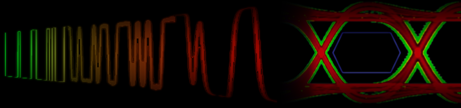
The scope of this work is to bring some of the signal processing tools to the verification environment. There are products, like USB2.0/3.0, that have available for download a software tool capable of analyzing the simulation waveforms and evaluate the circuit respects the standard specifications for interface signals. The major idea will be to create a similar software tool, without product limitations, capable of processing simulation saved files and evaluate if the previously defined parameters are met, like the signal processing software available inside the new digital oscilloscopes. It's also necessary to introduce new techniques for signal evaluation, in order to reduce the simulation time. On this work, Statistical Eye Diagram technique will be added to the software verification tool. The proposed software will add new features and will be open source code, this will allow the users to improved the existent libraries and the addition of new ones. The main characteristics are:

  • Proposed software will allow the end user to characterize and estimate the full ser/des architecture prior to the block implementation. This will reduce the number of simulation steps and the number of silicon re-spins
  • Silicon characterization without using third-part software will be allowed. User will need to use an oscilloscope to capture data, the data processing steps will be done of the proposed software. The need for third part characterization software will decrease
  • Proposed software will provide to the final user a set of functions/lybraries to help on jitter characterization/decomposition (Random Jitter, Periodic Jitter, Data Dependent Jitter)
  • Based on short but accurate transistor level simulations, silicon behavior will be accurately estimated
  • Secondary capabilities (nice to have)
    • Characterize hdmi/usb cables in terms of s-parameters
    • Characterize hdmi/usb cables in terms of noise characteristics
Proposed software will give to the end user the possibility of characterize all the analog characteristics with only one software (free and open source). It will allow the user to estimate and predict the product characteristics before silicon. Another major function will be the jitter/noise extraction without using third part software. Since the software will be developed in python it will allow the use across operating systems (Windows, Linux, MacOs). Jitter budget definition is always a hard task, with this software it will be easier. The end user will have the possibility of specifying the jitter budget for each major block and then evaluate if the overall target is achieved. It will be also possible to update the model with preliminary results obtained from simulations (after processing them with this software) to check if all blocks are under the internal specification. The addition of accurate cable models will allow the end user to better understand the overall effect on TX and RX sides. The must important functions are:
  • Clock recovery unit
  • Eye diagram generator
  • Statistical eye diagram generator
  • Analog to digital and digital to analog conversion
  • Measurement units
    • Rise and Fall times measurement
    • Minimum and Maximum values of the analog signal for each digital representation
  • Waveform generator
  • Data generation
    • Internally generated
    • Extracted from user .csv files
  • Random noise and duty cycle generation
  • Cable emulator
  • Equalization

Extent

The increasing growth on the Semiconductor Industry has pushed the High-Speed standards to other level, recent standards like USB3.0, PCI-E3.0, 10G XAUI, HDMI1.4 are examples of the new products being developed the DATA rate varies from 3.4Gbps on HDMI1.4 to 10Gbps on 10G XAUI. The demand for new high speed standards is driven by More's Law, More's Law describes the long term relation between number of transistors and time, in more detail following this law, the number of transistors that can be placed inexpensively on an integrated circuits doubles each 18 months. The processing capacity is directly related with the number of transistors, since the number of transistors is constantly increasing, the processing capacity increases as well, these will increase the demand for DATA that will end up in new data transfer standards that will operate at higher speeds.

The constant increase on the number of bits that can be processed per second (due to the increase on the processing capacity), lead to an increase on the number of bits that must be transferred between different integrated circuits. Since the inter-connection between integrated circuits is usually performed using LVDS interfaces (Low Voltage Differential Signaling), the Semiconductor Industry is always seeking for new High-Speed standards.

The DATA transferred across different IC needs to be effective, since the number of bytes shared across different IC increases, the number of errors allowed will reduce (in order to have an effective DATA transfer). There is a metric defined for the number of errors allowed by each DATA transfer. Such metric is defined as BER (Bit Error Rate), BER is defined as the number of bits transmitted with errors divided by the total number of transmitted bits, current standards have a typical value of 10e-12 (1 error per 1e12 of transmitted bits), recent standards are targeted to have a BER < 10e-15.

BER values are difficult to obtain in simulation, since the designer needs to transmitted billions of bytes to ensure that the design is in accordance with the specifications. The question is: How can a designer ensure that the design meets the targets within a reasonable simulation time? To achieve the targeted BER in simulation the designer will spend weeks or even months simulating the IC, this is not reasonable. It's necessary to use new methods to achieve this targets instead of capturing N*1e12 bits with a maximum of N errors detected to ensure that the a BER = 10e-12 is achieved. The major goal for each platform is to transmit a certain number of DATA on the shortest time and with the shortest number of errors.

High speed standards like: USB3.0, HDMI1.4,PCI-E3.0, SATA3.0, have defined a minimum BER, but there are more signal characteristics defined on those digital standards, like: Eye Diagram, Signal Amplitude, Rise/Fall times, High and Low voltage values, Jitter values, Resistor Termination values. Those standards include also protocol layers, interface pin description and pin functionalities, those functionalities can be easily verified trough fast digital simulations, the major difficulties are on the signal requirements, since that physical interface signals are dependent of the protocol layer, this dependence moves the simulation to a mixed-signal environment (digital and analog), the idea of verifying the analog and digital parts of the IC as separated blocks is no longer valid.